SOLARIS X
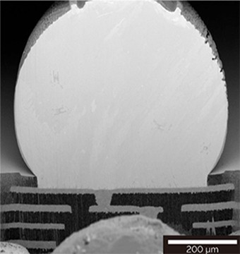
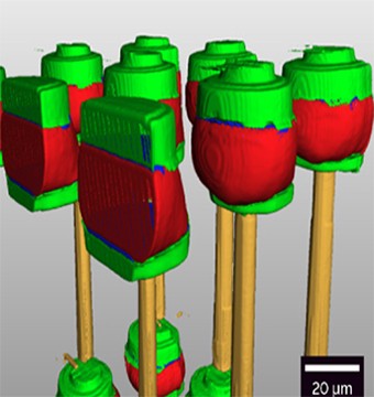
A Plasma FIB-SEM platform for deep sectioning and the highest resolution end-pointing for package level failure analysis
A Plasma FIB-SEM platform for deep sectioning and the highest resolution end-pointing for package level failure analysis
.jpg)
PRODUCT BROCHURE

SOLARIS X brochure
Extraordinary ultra-high resolution imaging and extremely fast micromachining. Download XEIA3 brochure!
PDF – 6.1 MB
KEY FEATURES
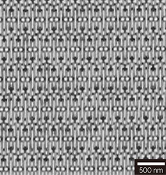
Triglav™ - newly designed UHR electron column
- - TriLens™ - objective system: unique combination of three-lens objective and crossover-free beam path
- - Advanced detection system with multiple SE and BSE detectors - TriSE™ and TriBE™
- - Triglav™ - Ultimate ultra-high resolution at low beam energy: = 0.9 nm at 1 keV and 0.6 nm at 15 keV
- - Electron beam currents up to 400 nA and rapid beam energy changes
- - Optimized column geometry for accommodating large wafers up to 8” and 12”
Specification
| Electron Optics | |
|---|---|
| Electron Gun | High brightness Schottky emitter |
| Resolution | |
| Standard mode In-Beam SE | 0.6 nm at 15keV |
Beam Deceleration Mode | 0.9 nm at 1 keV |
| Magnification at 30keV | 4 x - 1,000,000 x |
| Probe Current | 2 pA to 400 nA |
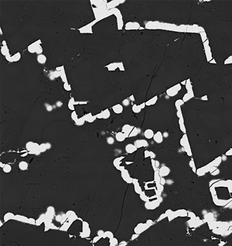
Extremely powerful Xe plasma FIB column
Xe plasma ion source FIB column for achieving the most challenging large-scale milling tasks in unbeatable short times frames
- - 50x faster than Ga LMIS FIBs.
- - on beam range current of 1 pA to 3 µA and resolution of < 12 nm
- - Newly developed high resolution Xe plasma FIB column achieving resolution of < 12 nm for extended patterning capabilities
- - Large-mass xenon ions with larger FIB current range for ultra-fast sputtering even without gas-assisted enhancement
- - Significant reduction in ion implantation compared to Ga LMIS FIBs
- - Rocking Stage - An effective and optimized polishing strategy against curtaining effect
Ion Optics
| Ion column | i-FIB+ 1.5v | |
|---|---|---|
| Ion Gun | Xe plasma ion source | |
| Accelerating voltage | 3kV to 30kV | |
| Probe current | 1 pA to 3 µA | |
| Resolution (at 30 keV) | < 12 nm | |
Magnification | Minimum 150 × at coincidence point and 10 kV (corresponding to 1 mm field of view), maximum 1,000,000 × 1 mm | |
SEM-FIB angle | 55° | |
Application
Semiconductors & Microelectronics
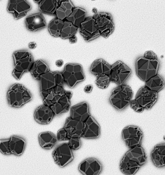
Material Science
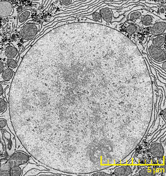
Life Sciences
Earth Sciences